Comprehensive Guide to Smart Home PCB Assembly Applications

Smart home technology is transforming how people interact with their living spaces. By 2025, over half of US consumers are expected to adopt these innovations, highlighting their growing importance. This surge reflects a desire for convenience, efficiency, and connectivity. At the heart of these advancements lies the PCB for smart home devices. These printed circuit boards serve as the control centers, enabling automation and communication among various systems. They integrate essential components like sensors and microcontrollers, ensuring seamless operation and enhanced functionality in modern homes.
Understanding PCB Assembly in Smart Homes
Printed Circuit Board (PCB) assembly plays a pivotal role in the functionality of smart home devices. It serves as the backbone for these advanced technologies, ensuring seamless operation and communication among various systems.
Basics of PCB Assembly
Components of PCB
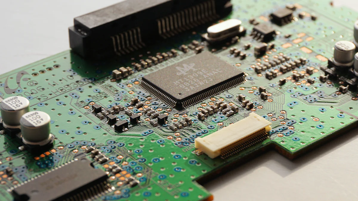
A PCB for smart home devices consists of several key components. These include:
Conductive Tracks: They connect different components, allowing electrical signals to flow.
Substrate: This is the base material that supports the entire structure.
Solder Mask: It protects the conductive tracks from oxidation and short circuits.
Silkscreen: This layer provides labels and markings for easy identification of components.
Each component contributes to the overall functionality and reliability of the PCB for smart home applications.
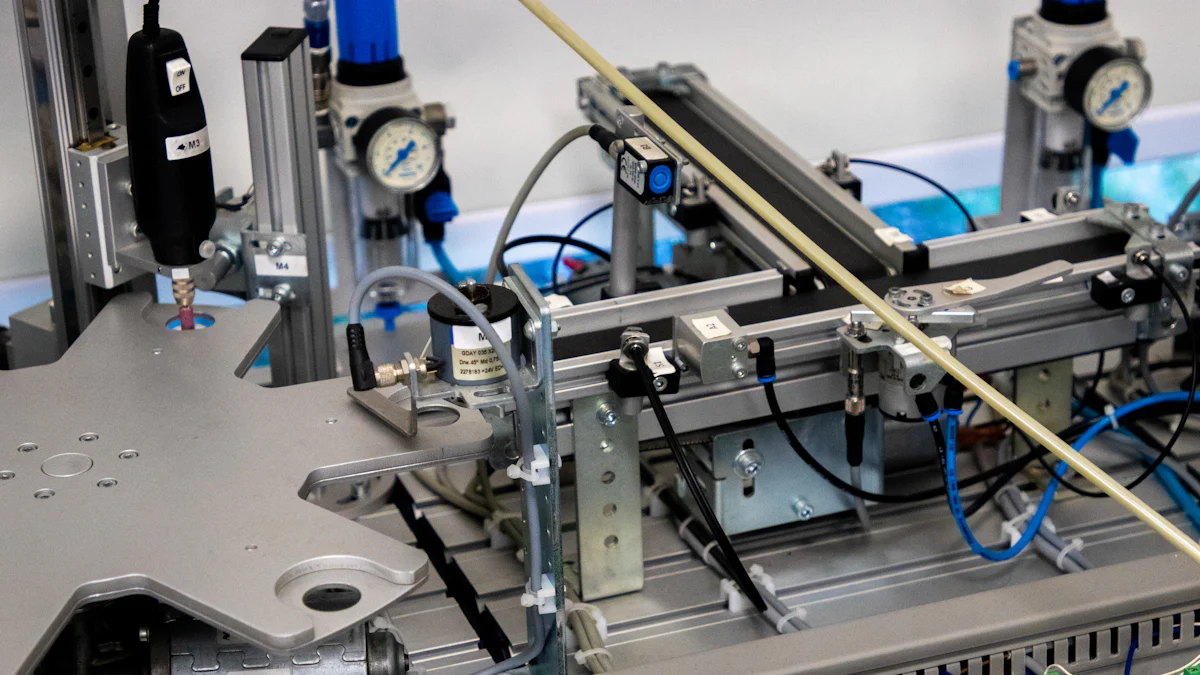
Assembly Process Overview
The assembly process of a PCB for smart home devices involves several steps:
Design and Layout: Engineers create a blueprint of the PCB, detailing the placement of components.
Printing: The design is printed onto the substrate using conductive materials.
Component Placement: Automated machines place components onto the board with precision.
Soldering: The components are soldered to ensure a secure connection.
Testing: The assembled PCB undergoes rigorous testing to verify its functionality and reliability.
This meticulous process ensures that each PCB for smart home devices meets high standards of quality and performance.
Importance in Smart Home Devices
Enhancing Device Functionality
A PCB for smart home devices enhances functionality by integrating various components into a single platform. It allows devices to perform multiple tasks efficiently. For instance, a smart thermostat can monitor temperature, adjust settings, and communicate with other devices, all thanks to its PCB.
Improving Energy Efficiency
Energy efficiency is a crucial aspect of smart home technology. A well-designed PCB for smart home devices optimizes power consumption. It ensures that devices use energy only when necessary, reducing waste and lowering utility bills. This efficiency not only benefits homeowners but also contributes to environmental sustainability.
Key Applications of PCB Assembly in Smart Homes
Smart home technology relies heavily on the PCB for smart home devices. These PCBs serve as the backbone for various applications, enhancing automation, security, and entertainment.
Home Automation Systems
Home automation systems benefit significantly from the PCB for smart home devices. They enable seamless control and integration of various functions.
Lighting Control
Lighting control systems use PCBs to manage and automate lighting throughout the home. They allow users to adjust brightness, set schedules, and even control lights remotely. This integration enhances convenience and energy efficiency, making homes more sustainable.
Climate Control
PCBs play a crucial role in climate control systems. They manage heating, ventilation, and air conditioning (HVAC) systems, ensuring optimal temperature and energy use. By integrating sensors and microcontrollers, these PCBs enable precise control and monitoring, contributing to a comfortable living environment.
Security and Surveillance
Security systems in smart homes rely on the PCB for smart home devices to provide robust protection and monitoring.
Smart Locks
Smart locks utilize PCBs to offer secure and convenient access control. They allow homeowners to lock and unlock doors remotely, monitor entry, and receive alerts. This technology enhances security while providing flexibility and ease of use.
Camera Systems
Camera systems in smart homes use PCBs to process and transmit video data. They enable real-time surveillance, motion detection, and remote viewing. The integration of advanced technologies within these PCBs ensures reliable and efficient security monitoring.
Entertainment Systems
Entertainment systems in smart homes are enhanced by the PCB for smart home devices, providing immersive experiences.
Audio Systems
Audio systems leverage PCBs to deliver high-quality sound throughout the home. They support wireless connectivity, allowing users to stream music from various devices. This integration creates a seamless and enjoyable audio experience.
Visual Systems
Visual systems, such as smart TVs and projectors, rely on PCBs to process video signals and connect with other devices. They enable features like voice control and content streaming, enhancing the overall entertainment experience.
The PCB for smart home applications forms the foundation for these innovative systems. By integrating various technologies, they ensure efficient, reliable, and user-friendly solutions that enhance modern living.
Types of PCBs Used in Smart Home Applications
Printed circuit boards (PCBs) form the backbone of smart home technology. Different types of PCBs cater to various needs and functionalities within smart home devices. Understanding these types helps in selecting the right PCB for smart home applications.
Single-Sided PCBs
Single-sided PCBs are the simplest type, featuring components on one side and conductive paths on the other.
Advantages and Disadvantages
Advantages:
Cost-effective: Single-sided PCBs are cheaper to produce, making them ideal for basic smart home devices.
Easy to design and manufacture: Their simplicity allows for quick prototyping and assembly.
Disadvantages:
Limited complexity: They cannot support complex circuits, restricting their use in advanced smart home applications.
Larger size: Single-sided PCBs often require more space, which can be a drawback in compact devices.
Multi-Layer PCBs
Multi-layer PCBs consist of multiple layers of conductive material, allowing for more complex designs.
Use Cases in Smart Homes
Advanced Functionality: Multi-layer PCBs support intricate circuits, making them suitable for sophisticated smart home systems like security and climate control.
Space Efficiency: They enable compact designs, essential for modern smart home devices where space is limited.
Multi-layer PCBs enhance the performance and reliability of smart home devices by accommodating more components and connections.
Flexible PCBs
Flexible PCBs offer versatility and adaptability, crucial for innovative smart home designs.
Benefits for Smart Devices
Flexibility: These PCBs can bend and twist, fitting into unconventional spaces and shapes. This flexibility is vital for wearable smart devices and appliances with unique designs.
Durability: Flexible PCBs withstand mechanical stress, enhancing the longevity of smart home devices.
Flexible PCBs contribute to the seamless integration and functionality of smart home systems, supporting the evolving landscape of smart technology.
The choice of PCB for smart home applications depends on the specific requirements and constraints of the device. By selecting the appropriate type, manufacturers can ensure efficient, reliable, and innovative solutions that enhance the smart living experience.
Challenges and Solutions in PCB Assembly for Smart Homes
Smart home technology continues to evolve, presenting unique challenges in the assembly of printed circuit boards (PCBs). Addressing these challenges is crucial for ensuring the reliability and efficiency of smart home devices.
Common Challenges
Miniaturization
Miniaturization stands as a significant challenge in the PCB assembly for smart homes. As devices become more compact, the demand for smaller PCBs increases. Engineers must fit numerous components into limited spaces without compromising functionality. This requires precise design and manufacturing techniques to maintain performance while reducing size.
Heat Management
Heat management poses another critical challenge. Smart home devices often operate continuously, generating heat that can affect performance and longevity. Effective heat dissipation methods are essential to prevent overheating and ensure device reliability. Engineers must design PCBs with materials and structures that facilitate efficient heat transfer.
Innovative Solutions
Advanced Materials
The use of advanced materials offers promising solutions to these challenges. Engineers now incorporate materials with superior thermal conductivity to enhance heat management. These materials help dissipate heat more effectively, maintaining optimal operating temperatures. Additionally, they support the miniaturization of PCBs by allowing for thinner and more compact designs.
Design Techniques
Innovative design techniques also play a vital role in overcoming PCB assembly challenges. Engineers employ sophisticated software tools to optimize PCB layouts, ensuring efficient use of space. Techniques such as in-line program systems streamline the assembly process, enhancing precision and reducing errors. These advancements contribute to the production of high-quality PCBs for smart home applications.
By addressing these challenges with innovative solutions, the industry can continue to advance smart home technology. The integration of advanced materials and design techniques ensures that PCBs meet the demands of modern smart home devices, providing reliable and efficient performance.
Future Trends in Smart Home PCB Assembly
Emerging Technologies
IoT Integration
The integration of the Internet of Things (IoT) in smart home PCB assembly is transforming how devices communicate and operate. IoT enables seamless connectivity among various home systems, enhancing automation and control. Engineers design PCBs to support IoT modules, allowing devices to interact and share data efficiently. This connectivity leads to smarter, more responsive home environments.
AI and Machine Learning
Artificial Intelligence (AI) and Machine Learning (ML) are revolutionizing smart home technology. PCBs now incorporate AI algorithms to enable devices to learn user preferences and adapt accordingly. For example, a smart thermostat can analyze usage patterns and adjust settings for optimal comfort and energy savings. This intelligent adaptation enhances user experience and efficiency.
Market Growth and Opportunities
Industry Projections
The smart home PCB market is poised for significant growth. Analysts predict a surge in demand as more consumers adopt smart technologies. This growth reflects the increasing desire for convenience and energy efficiency in residential settings. Manufacturers are investing in advanced PCB designs to meet these evolving needs, ensuring robust and reliable smart home solutions.
Investment Opportunities
Investment opportunities in smart home PCB assembly are expanding. Companies are exploring innovative materials and design techniques to enhance performance and reduce costs. Investors can capitalize on this trend by supporting research and development in cutting-edge PCB technologies. These investments promise substantial returns as the market continues to evolve and expand.
"Smart home PCB assembly plays a crucial role in enabling the automation, connectivity, and control of devices and systems within a smart home environment."
The future of smart home PCB assembly is bright, driven by technological advancements and market growth. By embracing these trends, the industry can continue to innovate and improve the smart living experience.
PCB assembly plays a vital role in smart homes, acting as the backbone for automation and connectivity. As technology evolves, exploring new advancements and applications becomes essential. Industry professionals must innovate and adapt to meet growing demands.
Customer Testimonial: "PCB Trace Technologies Inc. has always delivered top-notch quality, making them a reliable source for high-reliability applications."
By embracing these opportunities, the industry can enhance smart living experiences, ensuring efficiency and reliability in every home.
See Also
Optimizing Aerial Monitoring Using Analog FPV Thermal Imaging: An In-Depth Manual
Perfecting Aerial Thermal Scanning: A Detailed Tutorial with DroneThermal v4 Micro UAV Camera
Becoming Proficient in Aerial Thermal Camera Tech: The Definitive Manual for Choosing Top Drones
Achieving Mastery in Aerial Photography with Analog FPV Thermal Imaging: A Complete Handbook
Perfecting Aerial Thermal Imaging: A Comprehensive Manual for Drone Infrared Camera Technology
iSun digitech limited
iSun was established in 2007, specialising in automotive electronics, providing integrated software and hardware solutions. Products include Thermal imaging, Night Vision,Car Multimedia player, LCD Smart Car Key, CarPlay AI Box.

Contact Us: Ms. Coco Huang
E-mail: sales@iasun.cn
WhatsApp/Wechat: +86 13510421923